 | –≠–ª–µ–∫—Ç—Ä–æ–Ω–Ω—ã–π –∫–æ–º–ø–æ–Ω–µ–Ω—Ç: STW33N20 | –°–∫–∞—á–∞—Ç—å:  PDF PDF  ZIP ZIP |
STW33N20
N - CHANNEL ENHANCEMENT MODE
POWER MOSFET
s
TYPICAL R
DS(on)
= 0.073
s
AVALANCHE RUGGED TECHNOLOGY
s
100% AVALANCHE TESTED
s
REPETITIVE AVALANCHE DATA AT 100
o
C
s
LOW GATE CHARGE
s
HIGH CURRENT CAPABILITY
s
150
o
C OPERATING TEMPERATURE
s
APPLICATION ORIENTED
CHARACTERIZATION
APPLICATIONS
s
HIGH CURRENT, HIGH SPEED SWITCHING
s
SOLENOID AND RELAY DRIVERS
s
DC-DC CONVERTERS & DC-AC INVERTERS
s
TELECOMMUNICATION POWER SUPPLIES
s
INDUSTRIAL MOTOR DRIVES
INTERNAL SCHEMATIC DIAGRAM
ABSOLUTE MAXIMUM RATINGS
Symbol
Parameter
Val ue
Uni t
V
DS
Drain-source Voltage (V
GS
= 0)
200
V
V
DGR
Drain- gate Voltage (R
G S
= 20 k
)
200
V
V
GS
Gate-source Voltage
±
20
V
I
D
Drain Current (cont inuous) at T
c
= 25
o
C
33
A
I
D
Drain Current (cont inuous) at T
c
= 100
o
C
20
A
I
DM
(
∑
)
Drain Current (pulsed)
132
A
P
t ot
Tot al Dissipation at T
c
= 25
o
C
180
W
Derating Fact or
1. 44
W/
o
C
T
stg
St orage Temperature
-65 to 150
o
C
T
j
Max. Operat ing Junction Temperat ure
150
o
C
(
∑
) Pulse width limited by safe operating area
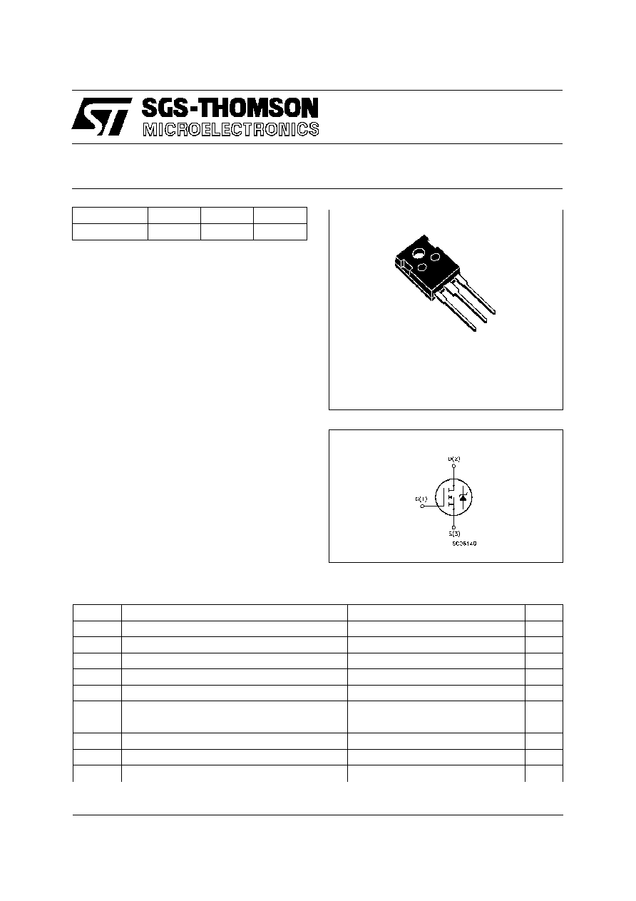
TYPE
V
DSS
R
DS(on)
I
D
ST W33N20
200 V
< 0.085
33 A
October 1997
1
2
3
TO-247
1/9
THERMAL DATA
R
t hj-ca se
R
t hj- amb
R
thc- si nk
T
l
Thermal Resistance Junction-case
Max
Thermal Resistance Junction-ambient
Max
Thermal Resistance Case-sink
Typ
Maximum Lead Temperature For Soldering Purpose
0.66
30
0.1
300
o
C/ W
oC/W
o
C/ W
o
C
AVALANCHE CHARACTERISTICS
Symb ol
Parameter
Max Valu e
Uni t
I
AR
Avalanche Current, Repetitive or Not -Repet itive
(pulse width limited by T
j
max,
< 1%)
33
A
E
AS
Single Pulse Avalanche Energy
(starting T
j
= 25
o
C, I
D
= I
AR
, V
DD
= 50 V)
600
mJ
ELECTRICAL CHARACTERISTICS (T
case
= 25
o
C unless otherwise specified)
OFF
Symb ol
Parameter
Test Cond ition s
Mi n.
Typ .
Max.
Un it
V
(BR)DSS
Drain-source
Breakdown Volt age
I
D
= 250
µ
A
V
GS
= 0
200
V
I
DSS
Zero G ate Voltage
Drain Current (V
GS
= 0)
V
DS
= Max Rating
V
DS
= Max Rating
T
c
= 100
o
C
10
100
µ
A
µ
A
I
GSS
Gate-body Leakage
Current (V
DS
= 0)
V
G S
=
±
20 V
±
100
nA
ON (
)
Symb ol
Parameter
Test Cond ition s
Mi n.
Typ .
Max.
Un it
V
GS(th)
Gate
Threshold
Voltage
V
DS
= V
GS
I
D
= 250
µ
A
2
3
4
V
R
DS( on)
St atic Drain-source On
Resistance
V
G S
= 10 V
I
D
= 16 A
0.073
0.085
I
D(o n)
On St ate Drain Current
V
DS
> I
D(on)
x R
DS(on) max
V
G S
= 10 V
33
A
DYNAMIC
Symb ol
Parameter
Test Cond ition s
Mi n.
Typ .
Max.
Un it
g
fs
(
)
Forward
Transconduct ance
V
DS
> I
D(on)
x R
DS(on) max
I
D
= 16 A
10
22
S
C
iss
C
oss
C
rss
Input Capacitance
Output Capacit ance
Reverse T ransfer
Capacitance
V
DS
= 25 V
f = 1 MHz
V
GS
= 0
3500
550
120
4500
700
160
pF
pF
pF
STW33N20
2/9
ELECTRICAL CHARACTERISTICS (continued)
SWITCHING ON
Symb ol
Parameter
Test Cond ition s
Mi n.
Typ .
Max.
Un it
t
d(on)
t
r
Turn-on Time
Rise Time
V
DD
= 100 V
I
D
= 16 A
R
G
= 4.7
V
G S
= 10 V
(see test circuit, figure 3)
25
50
40
70
ns
ns
(di/ dt )
on
Turn-on Current Slope
V
DD
= 160 V
I
D
= 33 A
R
G
= 4.7
V
G S
= 10 V
(see test circuit, figure 5)
800
A/
µ
s
Q
g
Q
gs
Q
gd
Total Gate Charge
Gate-Source Charge
Gate-Drain Charge
V
DD
= 160 V
I
D
= 33 A
V
G S
= 10 V
110
17
50
160
nC
nC
nC
SWITCHING OFF
Symb ol
Parameter
Test Cond ition s
Mi n.
Typ .
Max.
Un it
t
r(Vof f)
t
f
t
c
Of f-voltage Rise Time
Fall Time
Cross-over Time
V
DD
= 160 V
I
D
= 33 A
R
G
= 4.7
V
GS
= 10 V
(see test circuit, figure 5)
30
30
60
45
45
90
ns
ns
ns
SOURCE DRAIN DIODE
Symb ol
Parameter
Test Cond ition s
Mi n.
Typ .
Max.
Un it
I
SD
I
SDM
(
∑
)
Source-drain Current
Source-drain Current
(pulsed)
33
132
A
A
V
SD
(
)
Forward On Voltage
I
SD
= 10 A
V
GS
= 0
1.6
V
t
rr
Q
rr
I
RRM
Reverse Recovery
Time
Reverse Recovery
Charge
Reverse Recovery
Current
I
SD
= 33 A
di/dt = 100 A/
µ
s
V
DD
= 100 V
T
j
= 150
o
C
(see test circuit, figure 5)
400
5.6
28
ns
µ
C
A
(
) Pulsed: Pulse duration = 300
µ
s, duty cycle 1.5 %
(
∑
) Pulse width limited by safe operating area
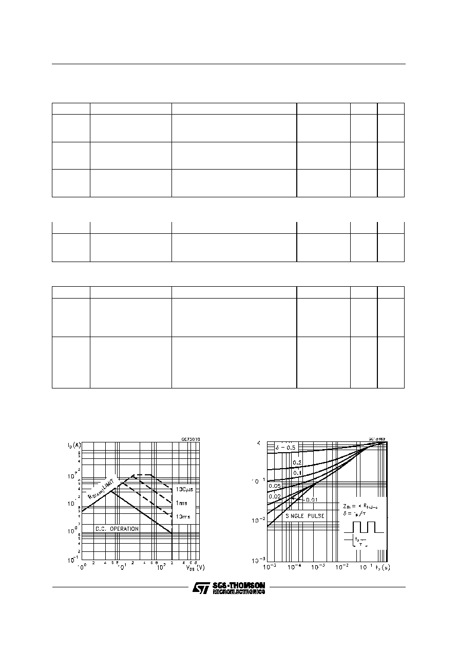
Safe Operating Area
Thermal Impedance
STW33N20
3/9
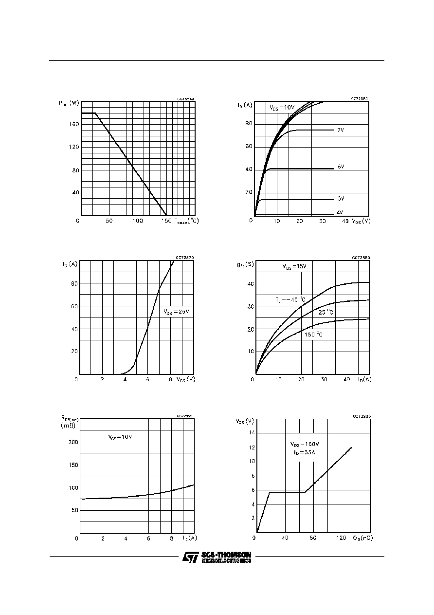
Derating Curve
Transfer Characteristics
Static Drain-source On Resistance
Output Characteristics
Transconductance
Gate Charge vs Gate-source Voltage
STW33N20
4/9
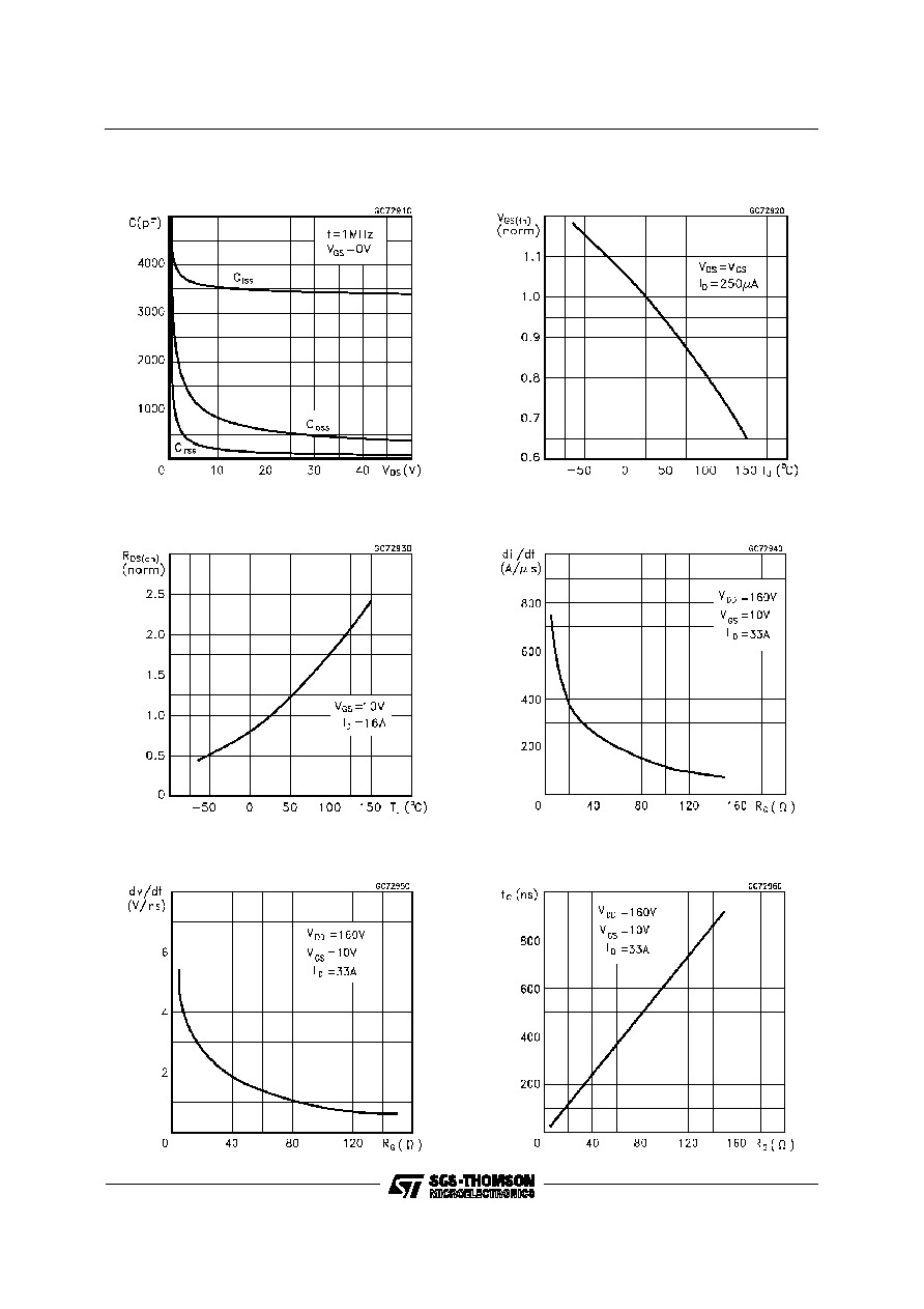
Capacitance Variations
Normalized On Resistance vs Temperature
Turn-off Drain-source Voltage Slope
Normalized Gate Threshold Voltage vs
Temperature
Turn-on Current Slope
Cross-over Time
STW33N20
5/9
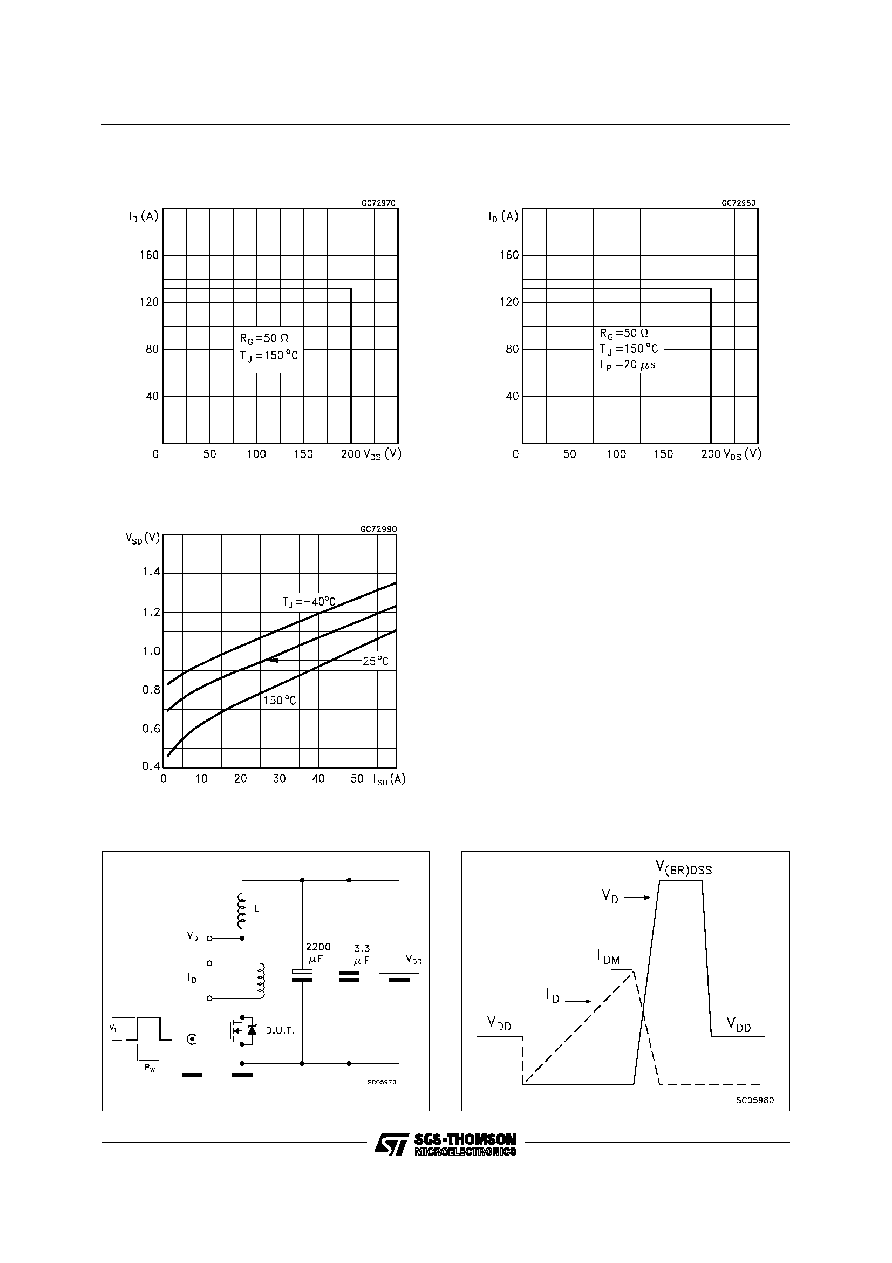
Switching Safe Operating Area
Source-drain Diode Forward Characteristics
Fig. 1: Unclamped Inductive Load Test Circuit
Accidental Overload Area
Fig. 2: Unclamped Inductive Waveform
STW33N20
6/9
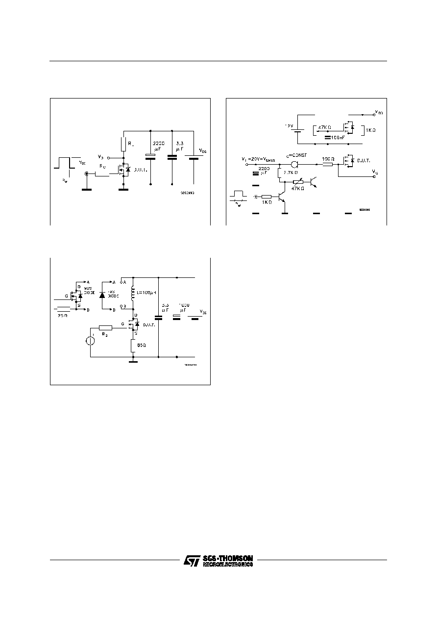
Fig. 3: Switching Times Test Circuits For
Resistive Load
Fig. 5: Test Circuit For Inductive Load Switching
And DIode Recovery Times
Fig. 4: Gate Charge test Circuit
STW33N20
7/9
DIM.
mm
inch
MIN.
TYP.
MAX.
MIN.
TYP.
MAX.
A
4.7
5.3
0.185
0.209
D
2.2
2.6
0.087
0.102
E
0.4
0.8
0.016
0.031
F
1
1.4
0.039
0.055
F3
2
2.4
0.079
0.094
F4
3
3.4
0.118
0.134
G
10.9
0.429
H
15.3
15.9
0.602
0.626
L
19.7
20.3
0.776
0.779
L3
14.2
14.8
0.559
0.413
0.582
L4
34.6
1.362
L5
5.5
0.217
M
2
3
0.079
0.118
Dia
3.55
3.65
0.140
0.144
P025P
TO-247 MECHANICAL DATA
STW33N20
8/9

Information furnished is believed to be accurate and reliable. However, SGS-THOMSON Microelectronics assumes no responsability for the
consequences of use of such information nor for any infringement of patents or other rights of third parties which may results from its use. No
license is granted by implication or otherwise under any patent or patent rights of SGS-THOMSON Microelectronics. Specifications mentioned
in this publication are subject to change without notice. This publication supersedes and replaces all information previously supplied.
SGS-THOMSON Microelectronics products are not authorized for use as critical components in life support devices or systems without express
written approval of SGS-THOMSON Microelectonics.
©
1997 SGS-THOMSON Microelectronics - Printed in Italy - All Rights Reserved
SGS-THOMSON Microelectronics GROUP OF COMPANIES
Australia - Brazil - Canada - China - France - Germany - Hong Kong - Italy - Japan - Korea - Malaysia - Malta - Morocco - The Netherlands -
Singapore - Spain - Sweden - Switzerland - Taiwan - Thailand - United Kingdom - U.S.A
. . .
STW33N20
9/9